RAD DATA COMMUNICATIONS
FCD-E1/1
|
Card Type |
E1 CSU/DSU |
|
Chip Set |
Unidentified |
|
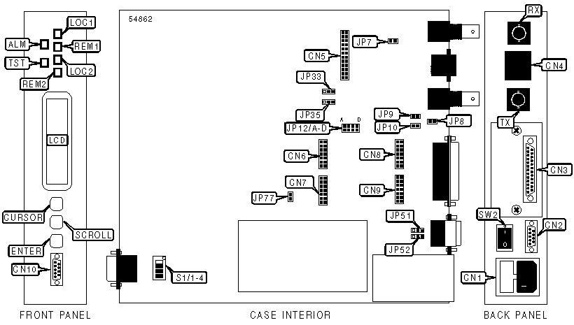
I/O Options |
AC power connector, 25-pin port (RS-530), BNC connectors (2), 9-pin serial ports (2 RS-232), E1 network interface via RJ-45 connector |
|
E1 Transfer Rate |
2.048Kbps |
|
E1 Protocol |
HDB3 |
|
Frame type |
CRC-4 |
|
Data Bus |
External |
|
CONNECTIONS | |||
|
Function |
Label |
Function |
Label |
|
AC power connector |
CN1 |
Header connector to CH2 interface board |
CN8 |
|
DTE serial port |
CN2 |
Header connector to CH2 interface board |
CN9 |
|
25-pin connector - channel 1 |
CN3 |
DCE serial port |
CN10 |
|
Network port via RJ-48 connector |
CN4 |
Power switch |
SW2 |
|
Header connector to sub interface board |
CN5 |
BNC connector - receive |
RX |
|
Header connector to CH2 interface board |
CN6 |
BNC connector - transmit |
TX |
|
Header connector to CH2 interface board |
CN7 | ||
|
USER CONFIGURABLE SETTINGS | |||
|
Setting |
Label |
Position | |
| » |
Signal ground is connected to the frame ground |
JP8 |
Closed |
|
Signal ground is not connected to the frame ground |
JP8 |
Open | |
| » |
Transmit side ground reference set for balanced interface |
JP9 |
Open |
|
Transmit side ground reference set for unbalanced interface |
JP9 |
Closed | |
| » |
Receive side ground reference set for balanced interface |
JP10 |
Open |
|
Receive side ground reference set for unbalanced interface |
JP10 |
Closed | |
| » |
Front panel push-buttons enabled |
JP77 |
Open |
|
Front panel push-buttons disabled |
JP77 |
Closed | |
| » |
Supervisor ports operate according to user-defined parameters |
S1/1 |
Off |
|
CSU/DSU uses default parameters stored in its EPROM |
S1/1 |
On | |
| » |
Default password enabled. Password=RAD |
S1/2 |
On |
|
User password enabled |
S1/2 |
Off | |
| » |
Loads user-selected parameters from NVRAM on power-up |
S1/3 |
Off |
|
Loads default parameters stored in its EPROM on power-up |
S1/3 |
On | |
| » |
Factory configured - do not alter |
S1/4 |
Off |
|
MAIN LINK INTERFACE | ||||||||
|
Function |
JP7 |
JP12/A |
JP12/B |
JP12/C |
JP12/D |
JP33 |
JP35 | |
| » |
Balanced interface |
Open |
Open |
Closed |
Open |
Open |
2 & 3 |
2 & 3 |
|
Unbalanced interface |
Closed |
Open |
Open |
Open |
Closed |
1 & 2 |
1 & 2 | |
|
Note: Pins designated are in the closed position | ||||||||
|
ALARM RELAY | |||
|
Function |
JP51 |
JP52 | |
| » |
Alarm relay disconnected. DTE port (CN2) provides full functionality |
2 & 3 |
2 & 3 |
|
Alarm relay connected instead of DCD and CTS lines |
1 & 2 |
1 & 2 | |
|
Note: Pins designated are in the closed position | |||
|
DIAGNOSTIC LED(S) | |||
|
LED |
Color |
Status |
Condition |
|
LOC1 |
Unidentified |
On |
Local synchronization lost on main link |
|
LOC1 |
Unidentified |
Off |
Local synchronization OK on main link |
|
REM1 |
Unidentified |
On |
Remote synchronization lost on main link |
|
REM1 |
Unidentified |
Off |
Remote synchronization OK on main link |
|
LOC2 |
Unidentified |
On |
Local synchronization lost on sub link |
|
LOC2 |
Unidentified |
Off |
Local synchronization OK on sub link |
|
REM2 |
Unidentified |
On |
Remote synchronization lost on sub link |
|
REM2 |
Unidentified |
Off |
Remote synchronization OK on sub link |
|
ALM |
Unidentified |
On |
Alarm condition detected on network |
|
ALM |
Unidentified |
Off |
Alarm condition not detected on network |
|
TST |
Unidentified |
On |
Device loopback test active |
|
TST |
Unidentified |
Off |
Device loopback test not running |

VER. X.21
|
CONNECTIONS | |
|
Function |
Label |
|
15-pin connector - channel 1 |
CN11 |

VER. V.35
|
CONNECTIONS | |
|
Function |
Label |
|
34-pin connector - channel 1 |
CN12 |
|
MISCELLANEOUS TECHNICAL NOTE |
|
CN11 and CN12 are modules which can be used to replace CN3, allowing for various DTE/DCE interfaces. |