TIARA COMPUTER SYSTEMS, INC.
LANCARD/A HIZ
|
NIC Type |
ARCnet |
|
Transfer Rate |
2.5Mbps |
|
Data Bus |
8-bit ISA |
|
Topology |
Linear Bus |
|
Wiring Type |
RG-62A/U 93ohm coaxial |
|
Boot ROM |
Available |
|
NODE ADDRESS |
||||||||
|
Node |
SW2/1 |
SW2/2 |
SW2/3 |
SW2/4 |
SW2/5 |
SW2/6 |
SW2/7 |
SW2/8 |
|
0 |
- |
- |
- |
- |
- |
- |
- |
- |
|
1 |
Off |
On |
On |
On |
On |
On |
On |
On |
|
2 |
On |
On |
On |
On |
On |
On |
Off |
On |
|
3 |
On |
On |
On |
On |
On |
On |
Off |
Off |
|
4 |
On |
On |
On |
On |
On |
Off |
On |
On |
|
251 |
Off |
Off |
Off |
Off |
Off |
On |
Off |
Off |
|
252 |
Off |
Off |
Off |
Off |
Off |
Off |
On |
On |
|
253 |
Off |
Off |
Off |
Off |
Off |
Off |
On |
Off |
|
254 |
Off |
Off |
Off |
Off |
Off |
Off |
Off |
On |
|
255 |
Off |
Off |
Off |
Off |
Off |
Off |
Off |
Off |
|
Note: Node address 0 is used for messaging between nodes and must not be used. A total of 255 node address settings are available. The switches are a binary representation of the decimal node addresses. Switch 1 is the Least Significant Bit and switch 8 is the Most Significant Bit. The switches have the following decimal values: switch 1=1, 2=2, 3=4, 4=8, 5=16, 6=32, 7=64, 8=128. Turn off the switches and add the values of the off switches to obtain the correct node address. (On=0, Off=1) |
||||||||
|
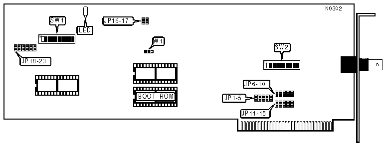
DIAGNOSTIC LED(S) |
||
|
LED |
Status |
Condition |
|
LED1 |
On |
Card is passing the token |
|
LED1 |
Blinking |
Card is reconfiguring |
|
LED1 |
Off |
Card is resetting or inoperative |
|
I/O BASE ADDRESS |
||||||||
|
Address |
SW1/1 |
SW1/2 |
SW1/3 |
SW1/4 |
SW1/5 |
SW1/6 |
||
|
|
160h |
On |
Off |
On |
Off |
Off |
On |
|
|
|
1E0h |
On |
Off |
Off |
Off |
Off |
On |
|
|
|
260h |
Off |
On |
On |
Off |
Off |
On |
|
|
» |
2E0h |
Off |
On |
Off |
Off |
Off |
On |
|
|
|
360h |
Off |
Off |
On |
Off |
Off |
On |
|
|
|
3E0h |
Off |
Off |
Off |
Off |
Off |
On |
|
|
|
Notes: An example of possible settings is shown. The switches are a binary representation of the hexadecimal I/O addresses. Switch 6 is the Least Significant Bit and switch 1 is the Most Significant Bit. The switches have the following decimal values: switch 6=1h, 5=2h, 4=4h, 3=8h, 2=10h, 1=20h. Turn off the switches, add the values of the off switches, and multiply the total by 10h to obtain the correct I/O address. |
|||||||
|
RIM BUFFER/BOOT ROM ADDRESS CONFIGURATION |
|||||
|
Buffer/Boot ROM Address |
SW1/7 |
SW1/8 |
SW1/9 |
SW1/10 |
|
|
|
1 x 00h |
On |
On |
On |
Off |
|
|
2 x 00h |
On |
On |
Off |
On |
|
|
3 x 00h |
On |
On |
Off |
Off |
|
|
4 x 00h |
On |
Off |
On |
On |
|
|
5 x 00h |
On |
Off |
On |
Off |
|
|
6 x 00h |
On |
Off |
Off |
On |
|
|
7 x 00h |
On |
Off |
Off |
Off |
|
|
8 x 00h |
Off |
On |
On |
On |
|
|
9 x 00h |
Off |
On |
On |
Off |
|
|
A x 00h |
Off |
On |
Off |
On |
|
|
B x 00h |
Off |
On |
Off |
Off |
|
» |
C x 00h |
Off |
Off |
On |
On |
|
|
D x 00h |
Off |
Off |
On |
Off |
|
|
E x 00h |
Off |
Off |
Off |
On |
|
Note: The variable x is configured in the next two tables. |
|||||
|
RIM BUFFER ADDRESS CONFIGURATION CONTINUED |
|||
|
Setting |
JP22 |
JP23 |
|
|
» |
x is set to 0 |
Open |
Closed |
|
|
x is set to 4 |
Closed |
Open |
|
BOOT ROM ADDRESS CONFIGURATION CONTINUED |
||||
|
Setting |
JP18 |
JP19 |
JP20 |
|
|
|
x is set to 4 |
Open |
Open |
Closed |
|
» |
x is set to 8 |
Open |
Closed |
Open |
|
|
x is set to C |
Closed |
Open |
Open |
Note: The Boot ROM occupies the upper 8K of the RIM buffer address, but can be relocated by changing these jumpers. The address given in the previous table then represents the Boot ROM address. |
||||
|
BOOT CONFIGURATION |
||
|
Boot attempt |
SW2/9 |
SW2/10 |
|
From network |
On |
On |
|
From floppy drive A, then network |
On |
Off |
|
From hard drive C, then network |
Off |
Off |
|
From floppy drive A, then from hard drive C, then network |
Off |
On |
|
INTERRUPT REQUEST |
|||||
|
IRQ |
JP1 |
JP2 |
JP3 |
JP4 |
JP5 |
|
2 |
Open |
Open |
Open |
Open |
Closed |
|
3 |
Open |
Open |
Open |
Closed |
Open |
|
4 |
Open |
Open |
Closed |
Open |
Open |
|
5 |
Open |
Closed |
Open |
Open |
Open |
|
7 |
Closed |
Open |
Open |
Open |
Open |
|
OPTIONAL TIMER INTERRUPT REQUEST 1 |
|||||
|
IRQ |
JP6 |
JP7 |
JP8 |
JP9 |
JP10 |
|
2 |
Open |
Open |
Open |
Open |
Closed |
|
3 |
Open |
Open |
Open |
Closed |
Open |
|
4 |
Open |
Open |
Closed |
Open |
Open |
|
5 |
Open |
Closed |
Open |
Open |
Open |
|
7 |
Closed |
Open |
Open |
Open |
Open |
|
OPTIONAL TIMER INTERRUPT REQUEST 2 |
|||||
|
IRQ |
JP11 |
JP12 |
JP13 |
JP14 |
JP15 |
|
2 |
Open |
Open |
Open |
Open |
Closed |
|
3 |
Open |
Open |
Open |
Closed |
Open |
|
4 |
Open |
Open |
Closed |
Open |
Open |
|
5 |
Open |
Closed |
Open |
Open |
Open |
|
7 |
Closed |
Open |
Open |
Open |
Open |
|
EXTENDED TIMEOUT CONFIGURATION |
||||
|
Response Time |
Reconfiguration Time |
JP16 |
JP17 |
|
|
» |
74.7µs |
840µs |
Open |
Open |
|
|
283.4µs |
1680µs |
Open |
Closed |
|
|
561.8µs |
1680µs |
Closed |
Open |
|
|
1118.6µs |
1680µs |
Closed |
Closed |
|
ON-BOARD RAM CONFIGURATION |
||
|
Size |
JP21 |
W1 |
|
No RAM installed |
Open |
Closed |
|
2KB |
Closed |
Pins 2 & 3 Closed |
|
8KB |
Closed |
Pins 1 & 2 Closed |