MICRO EXPRESS, INC.
FOREX 486 VESA (Rev. VL 421A/422)
|
Processor |
80486SX/80487SX/80486DX/ODP486SX/80486DX2 |
|
Processor Speed |
20/25/33/50(internal)/50/66(internal) |
|
Chip Set |
FOREX |
|
Max. Onboard DRAM |
32MB |
|
SRAM Cache |
64/128/256KB |
|
BIOS |
AMI |
|
Dimensions |
330mm x 218mm |
|
I/O Options |
32-bit VESA card slots (2) |
|
NPU Options |
None |
|
CONNECTIONS |
|||
|
Purpose |
Location |
Purpose |
Location |
|
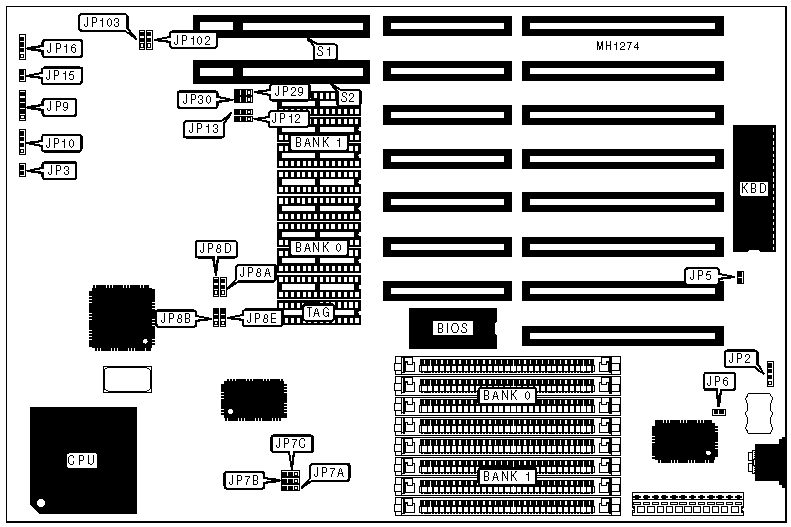
External battery |
JP2 |
Turbo switch |
JP15 |
|
Reset switch |
JP3 |
Turbo LED |
JP16 |
|
Power LED & keylock |
JP9 |
32-bit VESA local bus slots |
S1 & S2 |
|
Speaker |
JP10 |
|
|
|
USER CONFIGURABLE SETTINGS |
|||
|
Function |
Jumper |
Position |
|
|
» |
Battery select internal |
JP2 |
pins 1 & 2 closed |
|
|
Battery select external |
JP2 |
connected |
|
» |
Factory configured - do not alter |
JP5 |
closed |
|
» |
CMOS memory normal operation |
JP6 |
open |
|
|
CMOS memory clear |
JP6 |
closed |
|
|
VESA bus select zero wait states £ 33MHz |
JP102 |
pins 1 & 2 closed |
|
|
VESA bus select one wait state > 33MHz |
JP102 |
pins 2 & 3 closed |
|
|
VESA bus speed select £ 33MHz |
JP103 |
pins 1 & 2 closed |
|
|
VESA bus speed select > 33MHz |
JP103 |
pins 2 & 3 closed |
|
DRAM CONFIGURATION |
||
|
Size |
Bank 0 |
Bank 1 |
|
1MB |
(4) 256K x 9 |
NONE |
|
2MB |
(4) 256K x 9 |
(4) 256K x 9 |
|
4MB |
(4) 1M x 9 |
NONE |
|
5MB |
(4) 256K x 9 |
(4) 1M x 9 |
|
8MB |
(4) 1M x 9 |
(4) 1M x 9 |
|
16MB |
(4) 4M x 9 |
NONE |
|
20MB |
(4) 1M x 9 |
(4) 4M x 9 |
|
32MB |
(4) 4M x 9 |
(4) 4M x 9 |
|
CPU SPEED CONFIGURATION |
|||
|
CPU speed |
JP7A |
JP7B |
JP7C |
|
50MHz |
pins 2 & 3 closed |
pins 1 & 2 closed |
pins 2 & 3 closed |
|
33MHz |
pins 1 & 2 closed |
pins 1 & 2 closed |
pins 2 & 3 closed |
|
25MHz |
pins 1 & 2 closed |
pins 2 & 3 closed |
pins 1 & 2 closed |
|
20MHz |
pins 2 & 3 closed |
pins 1 & 2 closed |
pins 1 & 2 closed |
|
CPU TYPE CONFIGURATION |
||||
|
CPU Type |
JP12 |
JP13 |
JP29 |
JP30 |
|
80486DX2 |
pins 1 & 2 closed |
pins 1 & 2 closed |
pins 1 & 2 closed |
pins 1 & 2 closed |
|
ODP486SX |
pins 1 & 2 closed |
pins 1 & 2 closed |
pins 2 & 3 closed |
pins 2 & 3 closed |
|
80486DX |
pins 1 & 2 closed |
pins 1 & 2 closed |
pins 1 & 2 closed |
pins 1 & 2 closed |
|
80487SX |
pins 1 & 2 closed |
pins 1 & 2 closed |
pins 2 & 3 closed |
pins 2 & 3 closed |
|
80486SX |
pins 2 & 3 closed |
pins 2 & 3 closed |
pins 2 & 3 closed |
pins 2 & 3 closed |
|
SRAM CONFIGURATION |
|||||
|
Size |
Cache SRAM |
Location |
TAG |
JP8A & D |
JP8B & E |
|
64KB |
(8) 8K x 8 |
Banks 0 & 1 |
(1) 8K x 8 |
pins 2 & 3 |
pins 2 & 3 |
|
128KB |
(4) 32K x 8 |
Bank 0 |
(1) 8K x 8 |
pins 1 & 2 |
pins 1 & 2 |
|
256KB |
(8) 32K x 8 |
Banks 0 & 1 |
(1) 32K x 8 |
pins 2 & 3 |
pins 1 & 2 |
|
Note: Pins designated should be in the closed position. |
|||||