DIGITAL EQUIPMENT CORPORATION
DECPC LPX
|
Processor |
80486SX/80486DX/80486DX2 |
|
Processor Speed |
25/33/40/50(internal)/50/66(internal)MHz |
|
Chip Set |
Unidentified |
|
Video Chip Set |
None |
|
Maximum Onboard Memory |
64MB |
|
Maximum Video Memory |
None |
|
Cache |
128/256KB |
|
BIOS |
Unidentified |
|
Dimensions |
254mm x 218mm |
|
I/O Options |
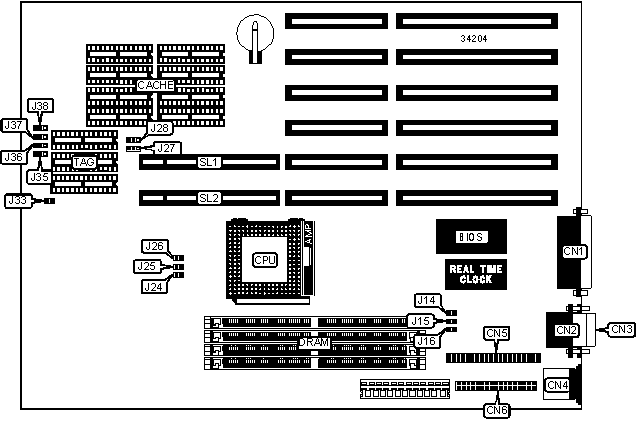
32-bit VESA local bus slots (2), floppy drive interface, IDE interface, parallel port, PS/2 mouse port, serial ports (2) |
|
NPU Options |
None |
|
CONNECTIONS | |||
|
Purpose |
Location |
Purpose |
Location |
|
Parallel port |
CN1 |
IDE interface |
CN5 |
|
Serial port |
CN2 |
Floppy drive interface |
CN6 |
|
Serial port |
CN3 |
32-bit VESA local bus slots |
SL1 & SL2 |
|
PS/2 mouse port |
CN4 | ||
|
USER CONFIGURABLE SETTINGS | |||
|
Function |
Label |
Position | |
|
» |
Flash BIOS normal operation |
J14 |
Open |
|
Flash BIOS recovery mode |
J14 |
Closed | |
|
» |
Monitor type select monochrome |
J15 |
Open |
|
Monitor type select color |
J15 |
Closed | |
|
» |
Factory configured – do not alter |
J16 |
Open |
|
» |
VLRDY >CPURDY connects to CPU bus ready |
J28 |
Pins 1 & 2 closed |
|
VLRDY >LRDY synchronized through chipset |
J28 |
Pins 2 & 3 closed | |
|
» |
Reset switch enabled |
J33 |
Closed |
|
Reset switch disabled |
J33 |
Open | |
|
DRAM CONFIGURATION | ||
|
Size |
Bank 0 |
Bank 1 |
|
4MB |
(2) 256K x 36 |
(2) 256K x 36 |
|
4MB |
(2) 512K x 36 |
None |
|
8MB |
(2) 1M x 36 |
None |
|
16MB |
(2) 2M x 36 |
None |
|
16MB |
(2) 1M x 36 |
(2) 1M x 36 |
|
24MB |
(2) 2M x 36 |
(2) 1M x 36 |
|
32MB |
(2) 4M x 36 |
None |
|
32MB |
(2) 2M x 36 |
(2) 2M x 36 |
|
40MB |
(2) 4M x 36 |
(2) 1M x 36 |
|
48MB |
(2) 4M x 36 |
(2) 2M x 36 |
|
64MB |
(2) 4M x 36 |
(2) 4M x 36 |
|
Note: The location of banks 0 & 1 are unidentified. | ||
|
CACHE CONFIGURATION | |||
|
Size |
Bank 0 |
Bank 1 |
TAG |
|
128KB |
(4) 32K x 8 |
None |
(3) 16K x 4 |
|
256KB |
(4) 32K x 8 |
(4) 32K x 8 |
(3) 16K x 4 |
|
CACHE JUMPER CONFIGURATION | ||||
|
Size |
J35 |
J36 |
J37 |
J38 |
|
None |
Open |
Open |
Open |
Open |
|
128KB |
Pins 1 & 2 closed |
Pins 1 & 2 closed |
Pins 1 & 2 closed |
Pins 1 & 2 closed |
|
256KB |
Pins 2 & 3 closed |
Pins 2 & 3 closed |
Pins 2 & 3 closed |
Pins 2 & 3 closed |
|
CPU SPEED SELECTION | |||
|
Speed |
J24 |
J25 |
J26 |
|
25MHz |
Closed |
Closed |
Open |
|
33MHz |
Closed |
Open |
Closed |
|
40MHz |
Open |
Open |
Closed |
|
50iMHz |
Closed |
Closed |
Open |
|
50MHz |
Open |
Open |
Open |
|
66iMHz |
Closed |
Open |
Closed |
|
VL BUS WAIT STATE SELECTION | ||
|
Setting |
J27 | |
| » |
0 |
Pins 1 & 2 closed |
|
1 |
Pins 2 & 3 closed | |