ADVANTECH CO., LTD
PCL-728
|
Card Type |
Analog output card |
|
Chip Set |
Unidentified |
|
Maximum Onboard Memory |
Unidentified |
|
I/O Options |
9-pin serial ports (2 RS-232) |
|
Hard Drives supported |
None |
|
Floppy drives supported |
None |
|
Data Bus |
8-bit ISA |
|
Card Size |
Half-length, half-height card |
|
CONNECTIONS | |||
|
Function |
Label |
Function |
Label |
|
9-pin serial port 1 |
CN1 |
9-pin serial port 2 |
CN2 |
|
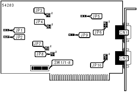
CHANNEL 1 SOURCE SELECTION | ||
|
Setting |
JP4 | |
| » |
Internal reference source |
Pins 3 & 4 closed |
|
External reference source |
Pins 1 & 2 closed | |
|
CHANNEL 2 SOURCE SELECTION | ||
|
Setting |
JP8 | |
| » |
Internal reference source |
Pins 3 & 4 closed |
|
External reference source |
Pins 1 & 2 closed | |
|
CHANNEL 1 INTERNAL VOLTAGE SELECTION | ||
|
Setting |
JP3 | |
| » |
-5V reference source |
Pins 3 & 4 closed |
|
-10V reference source |
Pins 1 & 2 closed | |
|
CHANNEL 2 INTERNAL VOLTAGE SELECTION | ||
|
Setting |
JP3 | |
| » |
-5V reference source |
Pins 3 & 4 closed |
|
-10V reference source |
Pins 1 & 2 closed | |
|
CHANNEL 1 POLARITY OUTPUT SELECTION | |||
|
Setting |
JP1 |
JP5 | |
| » |
Unipolar output enabled |
Pins 1 & 2 closed |
Pins 1 & 2 closed |
|
Bipolar output enabled |
Pins 2 & 3 closed |
Pins 2 & 3 closed | |
|
CHANNEL 2 POLARITY OUTPUT SELECTION | |||
|
Setting |
JP2 |
JP9 | |
| » |
Unipolar output enabled |
Pins 1 & 2 closed |
Pins 1 & 2 closed |
|
Bipolar output enabled |
Pins 2 & 3 closed |
Pins 2 & 3 closed | |
|
CHANNEL 1 CURRENT SINK RANGE SELECTION | ||
|
Range |
JP6 | |
| » |
4 - 20mA enabled |
Pins 3 & 5, 4 & 6 closed |
|
0 - 20mA enabled |
Pins 1 & 3, 2 & 4 closed | |
|
CHANNEL 2 CURRENT SINK RANGE SELECTION | ||
|
Range |
JP10 | |
| » |
4 - 20mA enabled |
Pins 3 & 5, 4 & 6 closed |
|
0 - 20mA enabled |
Pins 1 & 3, 2 & 4 closed | |
|
BASE I/O ADDRESS SELECTION | |||||||||
|
Setting |
SW1/1 |
SW1/2 |
SW1/3 |
SW1/4 |
SW1/5 |
SW1/6 |
SW1/7 |
SW1/8 | |
|
200h |
Off |
On |
On |
On |
On |
On |
On |
On | |
|
204h |
Off |
On |
On |
On |
On |
On |
On |
Off | |
|
208h |
Off |
On |
On |
On |
On |
On |
Off |
On | |
|
20Ch |
Off |
On |
On |
On |
On |
On |
Off |
Off | |
|
210h |
Off |
On |
On |
On |
On |
Off |
On |
On | |
| » |
300h |
Off |
Off |
On |
On |
On |
On |
On |
On |
|
3E0h |
Off |
Off |
Off |
Off |
Off |
On |
On |
On | |
|
3E4h |
Off |
Off |
Off |
Off |
Off |
On |
On |
Off | |
|
3E8h |
Off |
Off |
Off |
Off |
Off |
On |
Off |
On | |
|
3ECh |
Off |
Off |
Off |
Off |
Off |
On |
Off |
Off | |
|
3FOh |
Off |
Off |
Off |
Off |
Off |
Off |
On |
On | |
|
Note: A total of 125 valid base address settings are available. The switches are a binary representation of the decimal memory addresses. SW1/8 is the Least Significant Bit and switch SW1/1 is the Most Significant Bit. The switches have the following decimal values: SW1/1=512, SW1/2=256, SW1/3=128, SW1/4=64, SW1/5=32, SW1/6=16, SW1/7=8, SW1/8=4. Turn off the switches and add the values of the switches to obtain the correct memory address. (Off=1, On=0) | |||||||||